UPNOD 3: The RAM.
Posted on by Idorobots
After a lengthy break I'm back to the UPNOD series. This time we'll take a closer look at the dynamic random-access memory (DRAM) circuitry present on the PCB:
As usual, all of my findings can be found here.
RAM Chips
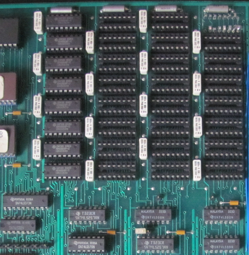
The circuit uses Hitachi-made HM4864-P3 65536-word x 1-bit Dynamic Random Access Memory chips organized in four banks of eight chips each. The manufacturer advertises them as:
- fast (200 ns access time),
- low power (330 mW active power).
I sure am glad that my Raspberry Pi runs on only a fraction of the total power this RAM requires - 10.56 freaking Watts - and that's not inclusive of the support circuitry. ( ͡° ͜ʖ ͡°)
In terms of operation these chips work similarly to the modern DRAM chips - requiring a periodic, externally triggered memory refresh cycle - except much, much simpler. There's no Double Data Rate (DDR), nor I/O channels and, of course, these are asynchronous. Basically, what we get to work with is a multiplexed address input and a couple of signal lines that control how the address input is interpreted:
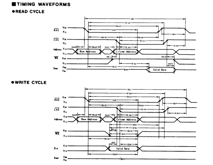
To read a memory location, we need to deassert the WE line, put the row address of the memory cell we wish to access onto the ADDRESS lines, assert the row address strobe line (RAS), put the column address onto the ADDRESS lines, assert the CAS line, wait for a while and, finally, we can read the Dout line. Of course, we have to deassert the CAS and RAS lines to end the memory read cycle. Memory write cycle is very similar, except we need to assert the WE line and present valid data onto the Din line before we assert the CAS line. The last memory operation we're interested in is the mandatory, periodic memory refresh cycle. There's nothing special to it, it's just a memory read cycle without specifying the column address - a so-called RAS-only refresh - as the chip refreshes entire rows at the same time.
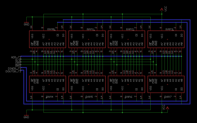
Single bits aren't generally useful for computation, so eight of these chips have to be combined to form a bank. Here's a schematic diagram of such a memory bank used in this telco card:
Often times, there is an additional, ninth chip present in each bank which is usually used for data parity checking. This design does not include one, so we can assume that error checking and recovery (if any) is performed in the software (if at all).
Support circuitry
Z80, the CPU that runs the entire thing, is an 8-bit microprocessor with a 16-bit wide address bus. This means it's not directly compatible with described RAM and needs quite a few glue-logic chips to actually make any use of the memory. In addition to multiplexing the address lines, this glue-logic is responsible for translating Z80 control signals (RD, WR, MREQ and REFSH) into RAM control signals (WE, RAS and CAS) and implementing various other features: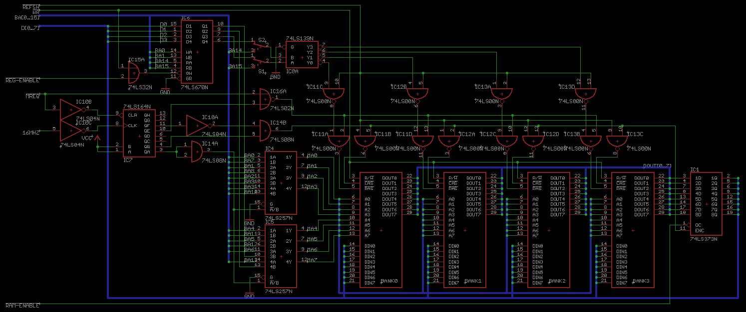
On the Z80 side, we have 16 lines of buffered address BA, data D, write enable WR, MREQ signaling a memory-based operation (contrary to IORQ signaling an IO operation) and RAM-ENABLE coming from the decoder circuit (described in a later post). BA goes to two 74LS257 selector chips via bank selection/mapping circuit described below. MREQ along with a 4*CLK oscillator signal go straight to a 74LS164 shift register which generates memory cycle steps:
- Initially, the lower half of the
BAaddress is selected on the74LS257selectors. - When
MREQis asserted so isRASand the cycle begins. - The first step selects the upper half of the
BAaddress. - The second step asserts the
CASline. - The third and fourth steps do not change anything.
- The fifth step deasserts the
RASline. - The sixth step deasserts the
CASline. - The remaining two steps again don't change anything.
Both RAS and CAS generators involve some basic 74XX series gates to facilitate RAM bank selection and memory refresh functionality. This is how a simulated version of this circuit performs:
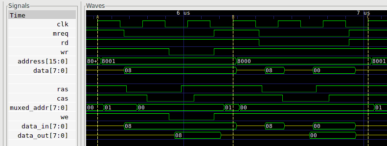
The first memory access (between A and B markers) shows a memory store operation. It looks fairly similar to the datasheet waveform except for the fact, that the WE line on the RAM is delayed quite significantly resulting in a so-called read-modify-write cycle - a single memory read that is closely followed by a memory write to the same location. Curiously enough, the value that is read during the read-modify-write cycle is completely ignored leading to the conclusion that it was either easier to implement, resulted in a more reliable memory refresh or allowed supporting more pin-compatible DRAM chips. I'm leaning towards the third option with a hint of the first one.
The second memory access (between B and C) shows a memory read operation. This time it looks nearly identical to the datasheet waveform if not for the stray values on the data_in line just after the MREQ is asserted... Wait what!? This is actually an artifact of the simulation software - what were seeing is the contents of the data_out latch from the previous cycle, since both the data_in line and the latched data_out are connected directly to the CPU data bus. We're seeing it because the data_out latch output is enabled too soon by the decoder circuit via the RAM_ENABLE line, however it quickly changes its contents, so this brief fluke seems not to interfere with the rest of the circuit in any way whatsoever.
The last part of the circuit is the aforementioned bank selection & mapping circuit based on a 74LS670 register file and a 74LS139 decoder. Basically, it works as an external IO device that can be written to with a 4-bit value. The upper two bits are used for RAM bank selection while the lower two bits add a constant offset to the currently mapped bank by virtue of two spare address lines going to the 74LS257-based address selector. Initially, 74LS670's registers are zeroed-out, so the system boots with the first RAM bank mapped to all four bank locations with no offsets. After booting, the OS is free to map each memory bank to each of the four locations under a specified offset, so in principle it could map a single bank to all four locations all at different offsets, or map four banks at four different locations with no offsets. Having such a configurable and mappable memory surely facilitated easy task switching in the primitive OS that runs on the card.
Memory refresh
Memory refresh circuitry relies heavily on the Z80's built-in refresh register and theREFSH signal. During each instruction decoding phase Z80 presents the contents of the 7-bit refresh register to the address bus and asserts the REFSH and MREQ lines. This happens to be enough to refresh the memory with little additional circuitry - as described above, RAS and CAS generators incorporate the REFSH signal using a handful of 74XX series logic gates. Here's a simulation of NOP-instruction decoding and accompanying refresh cycle: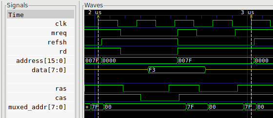
After the instruction opcode fetch (here resulting in 0xF3 value on the data bus) the REFSH signal is asserted, and shortly afterwards so is the MREQ signal. This results in a memory read operation taking place under the row address currently pointed to by the Z80 refresh register. The CAS generator circuit ensures that CAS lines on the RAM chips are not asserted as long as the REFSH line stays low - the specified row is refreshed, but no particular value is actually read.
This unique feature of the Z80 processor is very handy, but has a drawback - since memory is refreshed only when an instruction opcode is decoded, some sequences of long instructions might stall the memory refresh long enough to cause data corruption. For instance and for comparison with the NOP instruction above, here's a far "longer" DJNZ instruction:
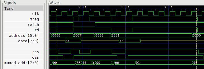
A sequence of DJNZ instructions performs a true memory refresh every 13 cycles and that's not even getting into Z80 instruction prefixes, which would place memory refresh cycles even further apart. As cute as it sounds, it probably never proved to be a problem in practice.
It would make for a neat factory-equipment-DoS plot for an episode of an 80' version of Mr. Robot, though... ¯\(ツ)/¯